Having your PCBs professionally manufactured is an important step towards bringing your product to market.
When you’re prototyping a new product that incorporates some kind of electronics on a printed circuit board (PCB), populating your boards by hand and soldering them on a repurposed electric hotplate works quite well. However, this manual process is far too slow and far too error prone to use for producing even a modest number of PCBs used for a product sold and shipped to customers or crowdfunding Backers.
For a product made available to the public, you will need to use a PCB assembly (PCBA) service to get not only your bare PCBs manufactured, but also to have all the components placed on the board and soldered. Many PCBA services also offer testing so that the correct function of each and every board can be verified before they arrive at your door to be integrated into your finished products.
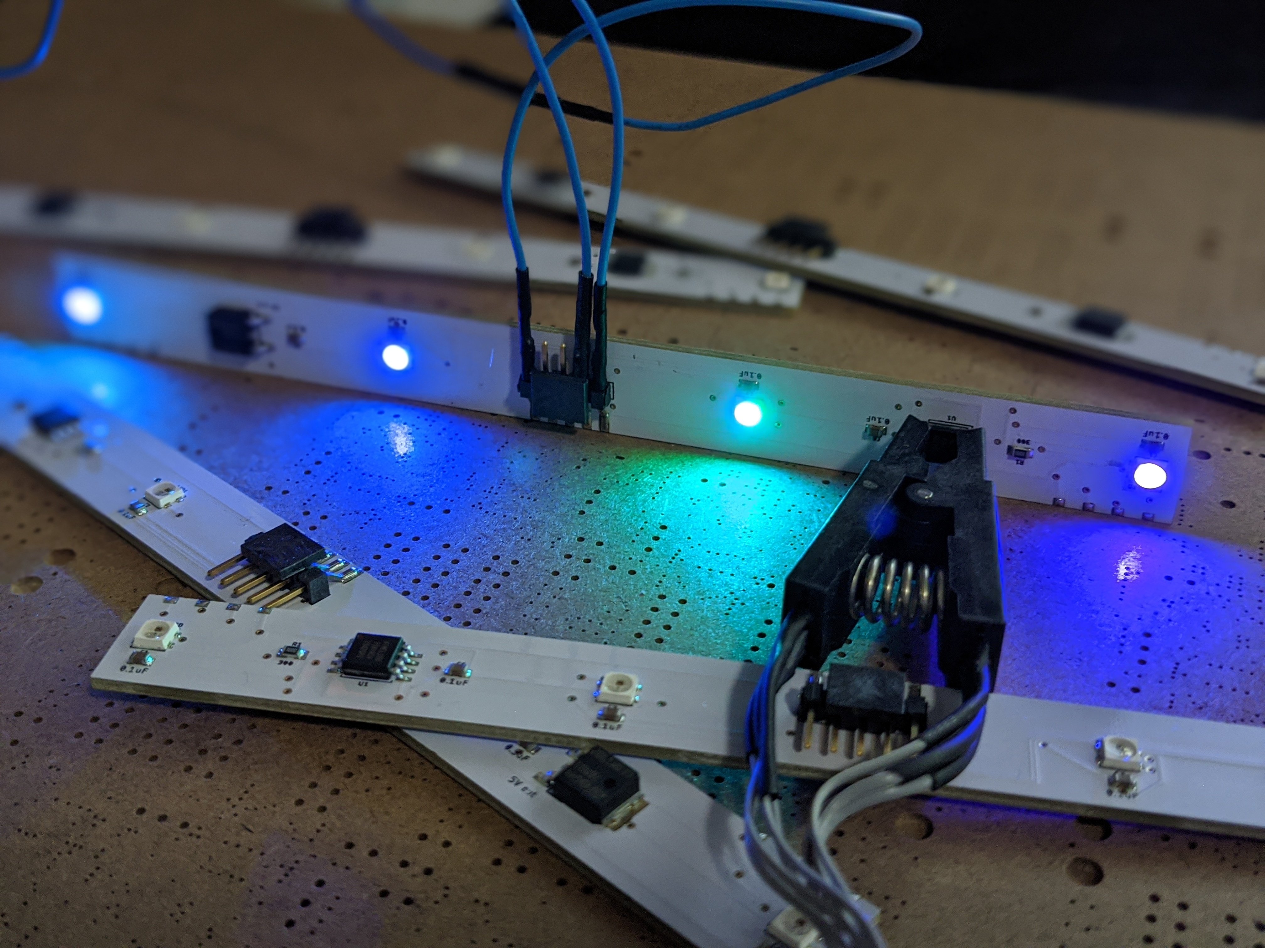
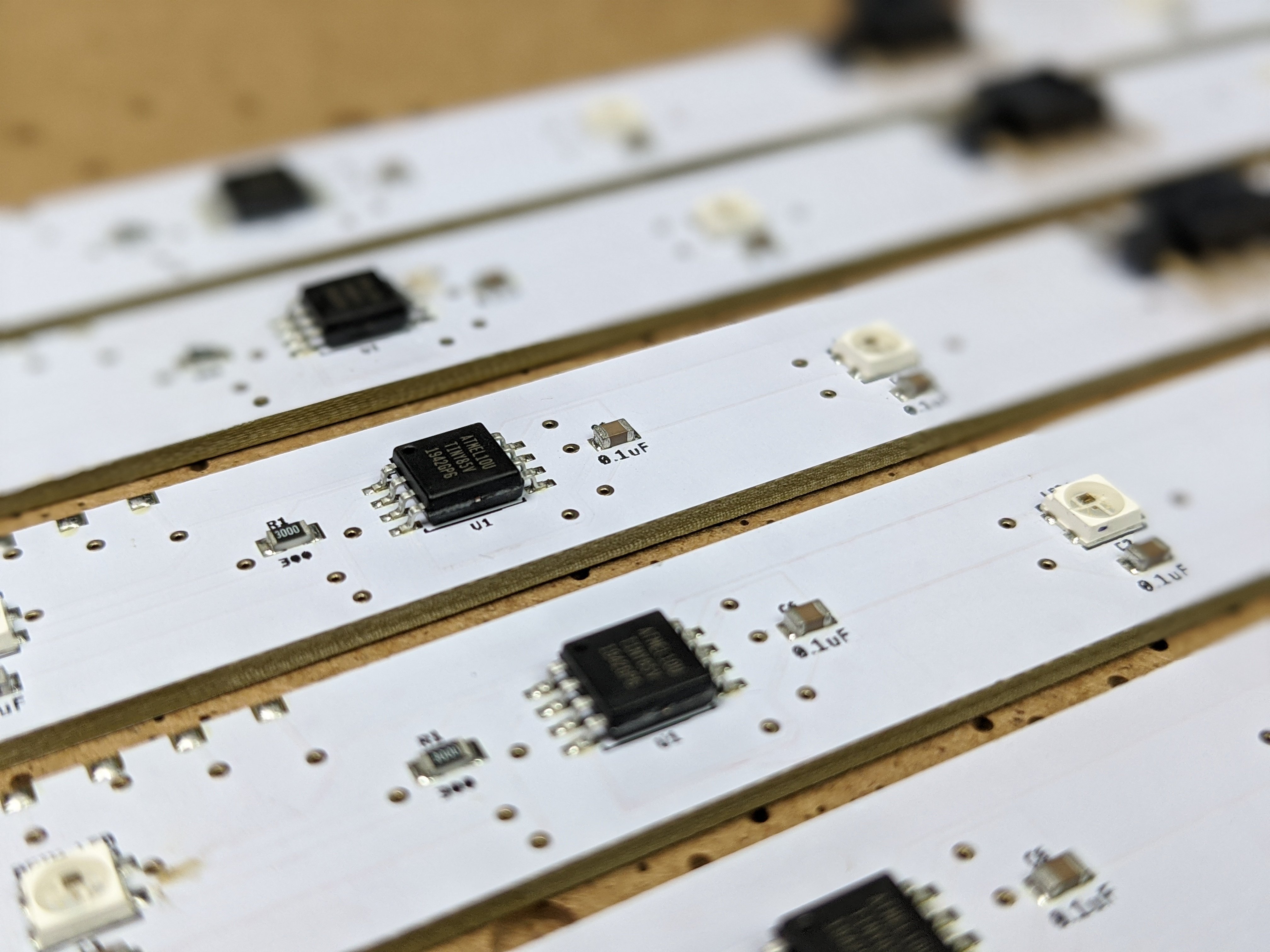
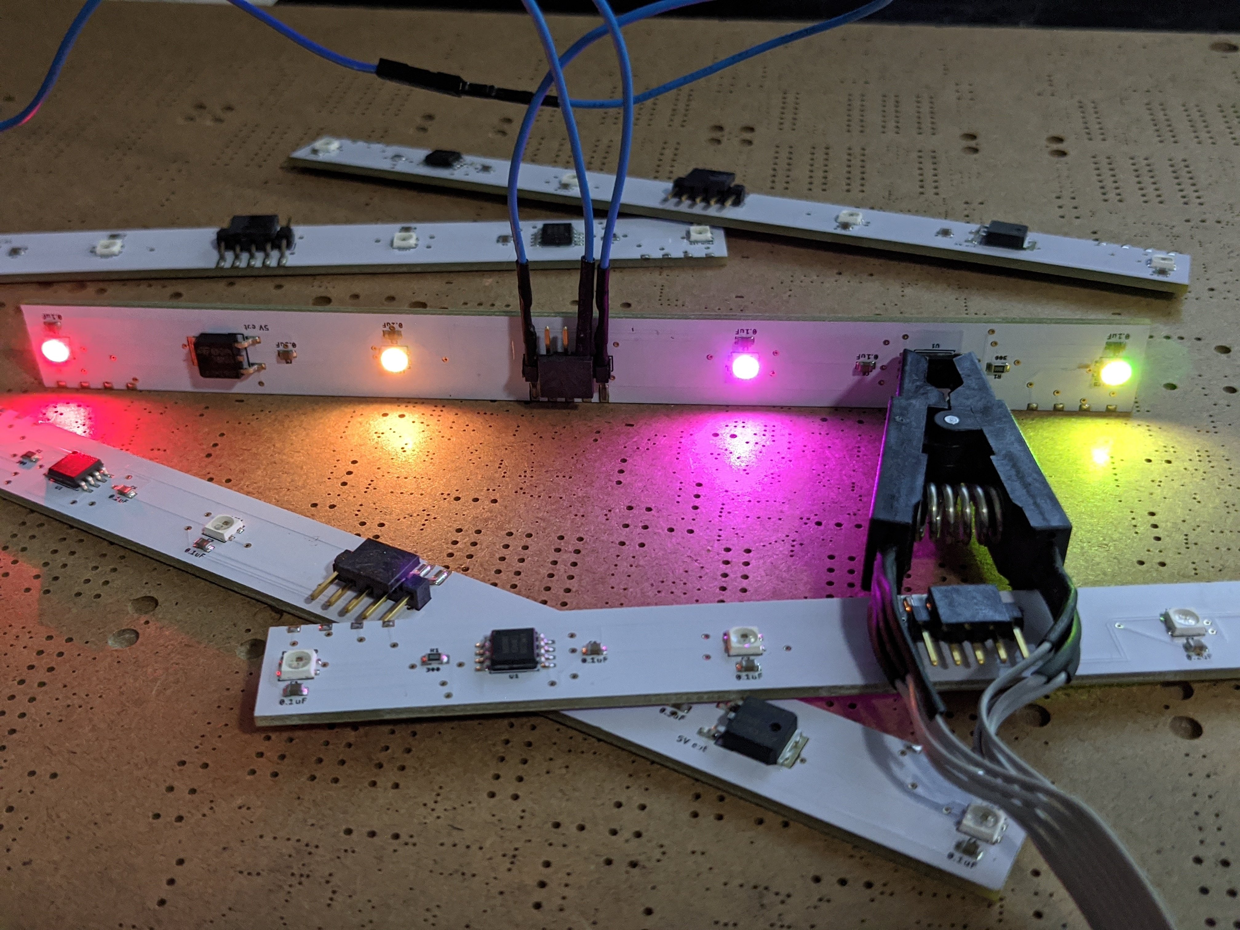
This is a LED controller module for a decorative lighting project. This PCB was manufactured and assembled by PCBWay.
This flowchart from Seeed Studio shows the steps involved in assembling a PCB.
On top of the already complex process of assembling bare PCBs, the assembly process introduces another collection of machines, technologies, and design considerations.
After the bare PCBs are made, solder paste is applied to the board with a machine resembling a silkscreen that uses a solder paste stencil to apply solder paste only to the pads on the PCB onto which electrical components will be mounted.
This is a semi-automated solder paste deposition machine used on Adafruit’s assembly line.
Typically, the boards are inspected in a variety of ways after each step of the assembly process. Some inspection stages are performed automatically using automated optical inspection (AIO) machines. These machines use a computer vision system to ensure, in this case, that each pad on the PCB has the correct amount of solder paste accurately applied.
Automated optical inspection machines are used to verify that the solder paste was applied correctly.
Then, a pick-and-place machine is used to quickly and accurately place SMT components onto the board. Pick-and-place machines are an amazing technology. The machines automatically retrieve individual components off reels, check the alignment of the components, and place them in the correct positions on the PCB. The fastest pick-and-place machines are capable of placing upwards of 50 components per second.
Pick-and-place machines grab parts, verify their alignment, and place them onto the PCB.
Then, the boards are passed through an oven that melts the solder paste and electrically connects all the components. The oven is designed to heat up and cool down the boards according to a specific heating curve. A conveyor belt carries the boards through the oven.
Inside the reflow oven, the boards pass through a series of temperature zones designed to heat and cool the boards along a specific curve.
All of the steps so far apply to SMT components. For through-hole components, the components themselves are typically placed by hand. Then, a solder wave machine is used to solder the legs of the PTH components on the underside of the board. The solder wave machine uses a small fountain of molten solder and quickly solders all the components. Thanks to the solder mask applied to the PCB, the molten solder only sticks to the component legs and PCB pads.
This is another machine used on the Adafruit production line to solder PTH components.
Finally, the boards go through a series of quality and functional testing steps. Just like with the solder paste, the assembled and soldered boards are inspected, either automatically or with human eyes, to make sure none of the parts were dislocated during the soldering process. The final step prior to shipping is, assuming it is provided by your PCBA manufacturer, functional testing. An automated machine, called an flying probe tester, tests every combination of pads to make sure all the connections match the reference design.
A flying probe tester verifies that the connections in the circuit match the design file
The video below, by Strange Parts on YouTube, is a tour of a printed circuit board assembly facility by a company called PCBWay. This is the service we will be using in this article for getting an example PCB manufactured.
Preparing Files for PCBA
You will need a collection of different files in order to place an order for printed circuit board assembly:
- A set of Gerber files are used to manufacture the bare PCB itself.
- A bill of materials (BOM) lists all the parts used in the design along with other information used to source the parts and correctly place them on the PCB.
- A centroid file (also called an insertion file, pick-n-place file, or XY data file) is used to program the machines used to assemble your PCB.
- Assembly drawings are used to verify your design, for manual assembly and soldering, for rework, and for testing.
- Photos of a finished prototype board can be generally helpful for clearing up any ambiguity in your design files.
Before starting the process of preparing the files necessary to have your design manufactured and assembled, you will, of course, need a completed design. In this tutorial, I am using the control unit for an LED lighting project called Borilux. The design work was done in Autodesk Eagle.
Beyond having the design completed though, it is wise to prototype your circuit as well. Between the cost of the actual boards, the cost of sourcing and possibly shipping components, the cost of assembly, the cost of preparing all the necessary files, and the shipping charges for getting your completed PCBs delivered, PCBA can involve a substantial investment. In addition, lead times for PCBA services and usually a couple weeks at least. Therefore, it is best to make certain your circuit design functions as expected before investing your time and money into PCBA.
Before investing in PCBA services, it is important to have a working prototype.
As a note, in this tutorial, I am using the PCB assembly services offered by a company called PCBWay. PCBWay is a popular PCB manufacturing company with extensive PCBA capabilities. Plus, PCBWay has very low minimum quantities for placing PCBA orders which is a benefit if you are working on late stage prototypes. The service does not force you to pay for a large number of prototype assembled PCBs that you may not need. The process for preparing files and placing an order with PCBWay should be very similar to other manufacturers. That said, you should always check your manufacturer's documentation to ensure you are preparing your design files and other assets according to their specifications
Generating Gerber Files
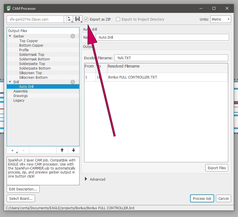
If you've ever had blank PCBs manufactured before, you probably have some experience with Gerber files. Plus, several other articles discuss generating Gerber files from a design in Autodesk Eagle. So, as a brief refresher, to generate Gerber files from a design in Eagle, first click on the CAM Processor button in the toolbar.
Next you will need to load a CAM job file that tells Eagle how to format your Gerber files according to your manufacturer’s specifications. Most PCBA services have a CAM file available for download. For ordering from PCBWay, I prefer using a profile developed by SparkFun electronics.
To download the job file, head over to the SparkFun Eagle Settings repository on GitHub. This repository contains a number of useful assets for use in Eagle, including some CAM profiles. I would recommend downloading the entire repository since you may wish to explore the other resources that SparkFun generously made available.
After extracting the .zip file, copy the sfe-berb274x-2layer cam file from the SparkFun_Eagle_Settings-master/cam directory and paste it into your Eagle cam directory. This is generally somewhere like Documents/eagle/cam.
Then, jump back into Eagle. In the CAM processor dialog box, in the Load Job File dropdown, if you are using PCBWay to get your electronics made, choose Open CAM File.
The last configuration option to choose before exporting the Gerber files is to ensure the Export as ZIP checkbox is selected.
Then, when you press the Process Job button, you simply need to choose a directory in which to store the .zip file that contains your set of Gerber files. These files will be used by PCBWay to create the bare PCB for your design.
Sourcing Parts
Before moving on to the next type of file needed to place a PCBA order for your design, the bill of materials, it is important to understand the different part sourcing options that are generally available for PCBA services. For companies like PCBWay, there are several ways the PCBA manufacturer can get the components needed to assemble your boards. The choice of how components and parts for your design are sourced affects a lot about your PCBA order: the lead time required to manufacture your boards, the cost per board, minimum order quantities, logistics costs, and any additional work that you may need to do before your PCBs can be assembled.
Consigned/Kitted
In a consigned part sourcing model, the PCBA customer purchases all of the components in the design and ships them to the PCBA manufacturer. The parts are put together in a “kit” so that a single package contains all the parts needed to manufacture the needed quantity of parts, along with paperwork listing all the parts the kit contains and information on the PCBA order to which the kit belongs.
A consigned part sourcing option can be attractive to product developers for a number of reasons. First and foremost, by keeping part sourcing in-house, developers can maintain a higher level of control over the design itself and over the manufacturing process. You, the product developer, can ensure that parts are ordered correctly and that there are no errors before passing the materials on for manufacturing. A second reason to choose consignment over other part sourcing options is if a design uses unique parts or parts that are difficult to obtain, it can be difficult for PCBA manufacturers to get the necessary parts themselves. A third reason developers might choose consignment is for the security of their intellectual property.
The primary downside of consignment part sourcing is the work involved on the part of the product developer. Tracking and monitoring inventory, handling international shipping, putting together kit documentation, and doing part purchasing all involves time and energy. In the case of in-development products, developers might prefer to use this time to continue working towards bringing a product to market rather than managing a supply chain.
Full Turnkey
Turnkey part sourcing is basically the opposite of consignment. With turnkey PCBA services, the manufacturer handles both the manufacturing PCBs and sourcing all of the necessary components. This option allows the entire manufacturing process, and part sourcing, to be outsourced. The product developer provides the PCBA manufacturer with a detailed bill of materials, and the manufacturer obtains all of the parts using their prefered vendors (typically large distributors like Mouser and DigiKey).
Turning over complete control of the manufacturing process and of supply chain management to the manufacturer is both a benefit and a disadvantage of turnkey part sourcing. For small teams of developers working towards bringing a product to market, turnkey sourcing allows time and energy to be spent on development, marketing, and sales rather than manufacturing. Turnkey part sourcing also allows companies to be more agile in responding to changes in market conditions or demand.
However, turn-key sourcing can also carry additional risks. Manufacturers may accidentally order incorrect parts due to misunderstandings in the design or accompanying documentation. Last, turnkey sourcing can be more expensive than using a consignment model because some PCBA manufacturers will charge a percentage of the total cost of parts and/or for the work involved in sourcing parts.
Partial Turnkey
Product developers can also choose to use a combination of consignment and full turnkey parts sourcing options. The important or less common parts of a PCB design can be purchased by the product developer and shipped to the manufacture, as in a consignment model, while commodity parts are sourced by the manufacturer. So, if you are developing a product with microcontrollers, LEDs, custom connectors, or other more important component, you can source those parts yourself while leaving the manufacturer to source things like capacitors, resistors, and other common components.
Creating a Bill of Materials
Another of the required files for getting your PCBs assembled is a bill of materials (BOM). The BOM lists each component used in your design, the reference designators for each part, manufacturer part numbers, and other information that allows the PCBA company to assemble your printed circuit board correctly according to your design. Obviously, this is all critical information when it comes to correctly assembling your PCB and sourcing parts.
Depending upon your strategy for part sourcing (consigned, full turnkey, or partial turnkey) your BOM will contain slightly different information. For PCBWay, the general information your BOM should include is summarized in the lists below. Keep in mind that your BOM will be reviewed by a member of the PCBWay team and if they have questions or require verification for any of the components in your BOM, they will reach out to you.
Consigned/Kitted Part Sourcing BOM
- Line#
- Quantity Per Part Number
- Reference Designator
- Part Number
- Part Description
- Package
- Type (Surface mount, Thru-hole or Hybrid)
Turn-key and Partial Turn-key Orders BOM
- Line#
- Quantity Per Part Number
- Reference Designator
- Part Number
- Part Description
- Package
- Type (Surface mount, Thru-hole or Hybrid)
- Manufacturers Name
- Manufacturers Part Number
- Distributors Part Number
Generating a BOM with Eagle
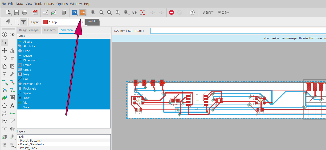
Depending upon how your project is organized, you may have a list of parts used to design your PCB, in which case, you can, of course, create the BOM for your PCBA manufacturer based on that list. However, if you do not have a list like that, you can use tools in Autodesk Eagle to export a BOM from your design. Specifically, we will use another ULP from the SparkFun Eagle Settings GitHub repository, the SparkFun-BOM_Generator.ulp. There is, in fact, a BOM generator ULP the ships with Eagle, but the SparkFun ULP is more flexible and easier to use.
To use the BOM, go to your BRD file, and click the Run ULP button in the toolbar.
Then, click the Browse button and select the SparkFun-BOM_Generator.ulp from the SparkFun Eagle Settings repository you downloaded earlier. Then, the dialog box for the ULP has two main sections. The one on the left shows all of the parts that will be included in the BOM. The panel in the middle shows the part designators that will not be added to the BOM. These latter parts will include things like wire pads that have designators but no actual components. You can move groups of parts back and forth between these sections to control which parts will appear in your BOM and which will not.
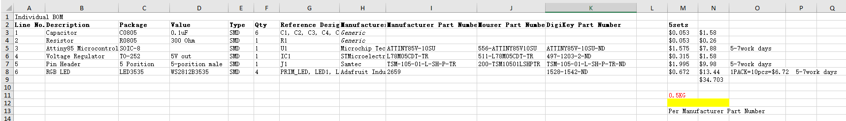
When you have your BOM list narrowed down, you can export the BOM as a CSV file.
Then you can easily import the CSV into Google Drive or Microsoft Excel and add any additional information you would like.
Generating Centroid Files
The final file that is required to place your PCBA order is one that goes by several names. A centroid file, also called a pick-and-place file or XY data file, lists each SMD part in your PCB by its reference designator, along with their coordinates, and rotation. For most PCBA manufactures, including PCBWay, you will need two centroid files for your board design. One for the top of the board, and one for the bottom. Even if your design does not have any components on the back side of the PCB, it can be a good idea to generate the centroid file for the back side anyway, just to add clarity.
All the information in centroid files is listed in a comma-separated list.
The centroid file is used by PCBA manufacturers to program pick-and-place machines. The file helps to ensure that each part is placed in the correct position and with the correct orientation on your board.
Generating Centroid Files in Eagle
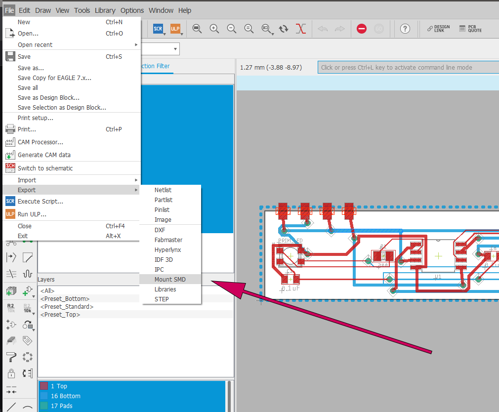
Generating centroid files in Eagle is extremely easy. Eagle includes a feature to export centroid files for your design. WIth your BRD file open, go to File > Export > Mount SMD.
Then, simply choose a location to save your pair of centroid files. You probably want both fiels saved to the same location.
Gather Supporting Materials
We’ve covered all of the files that are required to get your PCB manufactured and assembled: a set of Gerber files, the bill of materials, and a pair of centroid files. However, you can also provide additional information to help your PCBA company fully understand your design and the requirements for assembling your boards. These supporting materials do not have any standardized format, rather, you should concentrate on any additional documents that help to ensure there are no misunderstandings between you and your PCBA service because mistakes can be costly.
Assembly Diagrams
One useful supporting document that can help to make sure your PCBA manufacture fully understands where components on your PCB need to be mounted is an assembly diagram. This type of chart simply shows which components and which component values belong in different places on your PCB.
Prototype Photos
You’ve probably made more than a few prototype boards before moving on to PCBA. It can be useful to include a couple photographs of your prototype PCBs. These photos can be extremely helpful in helping your fab house sort out any questions that may arise from your design files alone.
Placing your PCBA Order with PCBWay
At this point, you have everything you need to place your PCBA order:
- Your Gerber files contain the information the fab house needs to make the PCBs themselves. Each individual Gerber file represents one layer of your design.
- The Bill of Materials lists all of the components in your design, along with their reference designators, and other information used to source parts.
- The centroid files allow your manufacturer to program their pick-and-place machines. The files list all the SMD components in your design and describe where the parts are to be mounted and in what orientation.
- Other materials you can optionally choose to provide, like assembly diagrams and photos of prototypes, can help your manufacturer fully understand your design. These files can help to avoid misunderstandings that can cause issues with your assembled boards.
Now that you have all these files, you can place your PCBA order. First, head over to PCBWay’s ordering page.
Ordering the Bare PCBs
The first section allows you to input all of the information needed for PCBWay to make your blank PCBs.
Parameter | Explanation |
|---|
Board type | The board type asks if your design files are for a single board or a panelized set of PCBs. For this tutorial, I am using Single pieces. If you are creating a panel, you can choose to design if yourself or have PCBWay design the panel. |
Different Design in Panel | If your design is not a panel, the answer to this field is 1. If you are making a panel, your panel might contain multiple copies of a single PCB design, or multiple different designs. |
Size | The size of your PCB is the size of the smallest rectangle that can fully enclose your design. A quick way of getting this information is on the Eagle Control Panel. |
Quantity | This is simply the quantity of bare PCBs you want made. This quantity will probably match the quantity of board to have assembled unless you have a reason for wanting both assembled and bare boards. |
Layers | This is the layer count of your PCB. Here, I have a 2 layer board. |
Material | This designates the material from which your PCBs will be made. In this article, I am using FR-4. |
FR4-TG | FR4-TG stands for “FR4 glass transition temperature.” This choice basically specifies the maximum temperatures your PCB substrate is design to withstand. TG 130-140 is the standard value. |
Thickness | PCBs can be made in various different thicknesses. 1.6mm is the most common thickness. |
Min Track/Spacing | This parameter basically specifies how fine the traces on your PCB are and how closely they are spaced. Using a tighter spacing will add cost. The typical value is 6/6mil. |
Min Hole Size | This parameter specifies the smallest hole diameter in the design. |
Solder Mask | You can get your PCB made in a variety of colors. Green solder mask has the best performance but you can choose to get your PCBs made in different colors for various different reasons. In this project, I chose White as my solder mask color because this project is for a LED lighting PCB. |
Silkscreen | You can also choose the color of the silkscreen for your PCB. Although, depending upon the color of your solder mask, you may not have a choice in silkscreen color. For example, if your solder mask is white, you cannot choose a white silkscreen. |
Gold fingers | Gold fingers are a specific design feature used to allow a PCB to be plugged into a socket. You may be familiar with this design feature if you’ve ever assembled a PCB. Graphics cards and other PCI devices have gold fingers to plug into the motherboard. |
Surface finish | For all of the SMD pads and plated through-holes on your PCB, there are several different technologies for applying a finish to these contact points. For this design, I am using HASL lead free because it is inexpensive, but also does not contain lead. |
Via Process | You can generally ignore this parameter because Eagle specifies a via process and PCBWay will use that setting even if you choose a different option on the ordering page. |
Finished copper | This parameter specifies the thickness of the copper layer on the plated FR-4 from which your PCB will be made. The thickness of copper is expressed as a weight of metal per square foot of board area. The default value is 1 oz Cu. |
Extra PCB product number | PCBWay will print a number on your PCB that allows them to identify and track your boards through the manufacturing and assembly processes. If you want this number omitted, there is an extra charge. |
In the Eagle Control Panel, the size of your PCB will be displayed when you select the .brd file.
These are gold fingers. They are used in some kinds of board-to-board connectors.
You can, of course, adjust any of these settings according to the requirements for your project.
Ordering PCB Assembly
Once you’ve input all the information needed for PCBWay to manufacture your actual PCBs (except, of course, your Gerber files, which will be uploaded in the next page), you can move on to placing your PCB assembly order. At the bottom of the PCBWay ordering page, there is a checkbox for selecting Assembly Service.
When you check the box, you will be presented with another set of parameters to configure for your PCBA order.
Parameter | Explanation |
|---|
3 flexible options | First, you can select the type of part sourcing to use, as discussed above. In this case, I am using the Turnkey service. |
Board type | Next is the type of board you want to have assembled. This parameter should be set to match the Board Type parameter in the above section. |
Assembly side | You will also choose which side of your PCB has components mounted to it, the top size, the bottom side, or both sides. |
Quantity | You will again select the order quantity. This parameter will probably match the quantity parameter from above. |
Number of unique parts | This parameter specifies the total number of different types of components in your design. This parameter does not indicate the total number of parameters, just the number of different types... |
Number of SMT parts | ...this parameter indicates the gross number of SMT parts in your design. |
Number of through-hole parts | You will also indicate how many PTH components your design uses. |
Once you’ve input and double-checked all the information on this ordering page, click the Calculate button.
The final bits of information, on the right side of the ordering page, is for selecting your PCB build time. The standard build time is 3-4 days but you can choose to expedite your PCBA order. Note that the build time does not include the time required for PCBWay to obtain your parts, whether you are shipping parts to the company or if you selected the turnkey option. Also note that the final price presented does not include the cost of components if you select turnkey as your part sourcing option.
Uploading Design Files
Now that you have all the information about your design files entered into the PCBWay ordering system, you can enter the design files themselves. There are three image file upload buttons. The first is for your Gerber files in a .zip archive. The second is for your BOM in Excel format or CSV. The third is for your centroid files, along with extra files, in a .zip archive.
Once you have all the files submitted, the next step is to wait for the team at PCBWay to review your order. As part of the review process, PCBWay will verify that there are no issues with any of your Gerber or centroid files, or any other issues with any of the other information you provided. In case there are any issues, PCBWay will contact you via email.
Review BOM Costs for Turnkey or Partial Turnkey Orders
If you decide to use turnkey or partial turnkey part sourcing, you will receive an updated version of your BOM a day or two after you place your order with pricing for each of the components in your design, along with the lead time required for PCBWay to get your parts.
You will be able to review this BOM and make any necessary changes before giving your approval for PCBWay to continue with manufacturing and assembling your boards. WIth this updated BOM, you will be able to calculate the exact cost of getting your boards made. The cost will be the price you paid when placing your order, plus the cost of the components in this BOM.
Confirm Assembled Boards before Shipping
The final step in getting your PCBs manufactured and assembled by PCBWay happens just before PCBWay ships your boards. Once your PCBs have been manufactured and assembled, PCBWay will send you an email with photos of your finished boards. This gives you the opportunity to give the boards your final approval before they get shipped out. You will want to double check all the components have been installed in the correct places and in the correct orientation.
Once you approve the finished boards, your fully assembled PCBs will be on their way to your door.
Conclusion
Moving from assembling your PCBs yourself by hand to having them professionally made by a PCB assembly company like PCBWay is an essential step towards bringing a new product to market. If you’ve already had a few prototype PCBs made, the process of getting your boards assembled only involves creating a few additional files.
File | Purpose |
|---|
Gerber Files | This set of files gives your PCBA manufacturer the information needed to make your blank PCBs. |
Bill of Materials | This is a list of components in your design, along with reference designators. |
Centroid Files | This pair of files is used to program pick-and-place machines so they know where each of the components in your design belong and in what orientation they should be mounted to your boards. |
Supporting Materials | These optional files can include assembly diagrams, photos, or other resources that will help ensure there are no miscommunications between you and your PCBA manufacturer. |
As part of getting your PCBs professionally manufactured, you will also need to decided on a part sourcing method. There are several ways your PCBA manufacturer can get all the components needed to build your design.
Part Sourcing Method | Description |
|---|
Consigned/Kitted | One option is for you to get all the components needed for your design yourself, package them up, and send them all to your PCBA manufacturer. |
Full Turnkey | Some PCBA manufacturers, like PCBWay can handle all of the part sourcing for you. |
Partial Turnkey | You can go with a combination of consigned and turnkey part sourcing. Generally this involves sourcing the more important parts of your design yourself, and leaving your PCBA manufacturer to source the more common parts. |
Using a professional PCBA service will allow you to scale your production to accommodate however many orders you need to fulfil without creating a bottleneck by building the electronics yourself or risking the quality of your product