Maker Pro
Maker Pro

Digital programmable CDI ignition for 2-stroke engines

bob weir

Sep 10, 2014
235
Joined
Sep 10, 2014
Messages
235
DSC00386.JPG DSC00386.JPG

all leds are lit . thus ADRES = FF or 255 decimal. the time base is 200uS / div
so the time between edges is about 800 uS. 800 / 255 = 3+ uS per ADRES unit
 

bob weir

Sep 10, 2014
235
Joined
Sep 10, 2014
Messages
235
... some thoughts about the fotos yesterday and a little math ...3F = 200 uS delay and FF = 800uS
delay and FF / 3F = 4 and 800 / 200 = 4 , roughly ... as a little confirmation that the delays are linear with the pot-ADRES-led count.

also ... about trying to buy a good cdi-ignition from the yamaha dealer ... none i spoke
with had the means to test those items out-of-the-box . in other words they lacked
a simulator that would do what the '506 code is doing. so , again , that policy is buyer beware for the diy'r. you roll the dice . the replacement parts could of worked.

or one can simply hire them to do the installation. and let the burden of the parts working
be for them to bear. this move could have worked too. but then
i'd have 1) paid a lot more and 2) missed out on all the
challenge and education that comes from tackling a new project like this one has become.

along the way when i realized this effort was going to take awhile i searched for and
found a good used dirt bike to have in the interim. it sucked not having a bike to ride.
 
Last edited:

bob weir

Sep 10, 2014
235
Joined
Sep 10, 2014
Messages
235
below is the flow diagram for the test code in the 16F506 uC . plus sketches of the circuit
and output signals.

the next step is testing it against the code in the 12F508 uC . so cross your fingers
that goes well. i'm ready for this project to be done with.


506 tst code flow diag apr 18 001.jpg
 

bob weir

Sep 10, 2014
235
Joined
Sep 10, 2014
Messages
235
and now the assembly listing source code loaded into the 506 chip.

running and testing the code led to these results :
i got 32.0 uS delay per unit of w for w = 50 , 100 and 150 using the MPASM stopwatch.
and on the scope was measured 1640 , 3250 and 4800 uS for the same 50 , 100 and 150 w-values .

note something new with this 506 uC code not seen with the 508 uC. being how it has 1024 ml's
that means 2 pages. and the goto and call instructions now need a 'pagesel' . and the 506 has 67
ml's for user variables.. by the documentation on p. 16 you can see these are spread out among
the 4 banks . so banksel is needed too. here though my understanding falls short. this test code
has only 6 variables in the UDATA section. and by p. 16 you can see there are 3 + 16 = 19 ml's.
so the 6 variables can all fit into bank 0 with room to spare. thus no banksel were used. and no
error msg's occurred during the build step . the usage of pagesel and banksel is an area of
active reading and learning.
 

Attachments

  • 506 test code apr 18 p 1 of 3 001.jpg
    506 test code apr 18 p 1 of 3 001.jpg
    171.5 KB · Views: 174
  • 506 tst code p 2 of 3  apr 18 001.jpg
    506 tst code p 2 of 3 apr 18 001.jpg
    196.4 KB · Views: 171
  • 506 tst code p 3 of 3  apr 18 001.jpg
    506 tst code p 3 of 3 apr 18 001.jpg
    104.3 KB · Views: 157
Last edited:

bob weir

Sep 10, 2014
235
Joined
Sep 10, 2014
Messages
235
testing of the 16F506 uC and the 12F508 uC together has begun. here are 2 scope images
from that testing effort.

making sense of them is more challenge. as the images show the story of what the
code is actually doing. instead of what i was expecting to see.
the jury is still out on them both.

it all needs further study. i just wanted to post this as a sample of what the
final say on the code being good or not will look like


this scope image shows CH 1 = -71 pulse CH 2 = -10 pulse and CH 3 = fire pulse
after the 506 & 508 have been running awhile. the pot/leds is set for ADRES = FF
the fire pulse is about .005 s after the -71 pulse LE . and occurs before the -10
pulse , so in general that much looks good.


apr 20 single start adres = FF.jpg
 
Last edited:

bob weir

Sep 10, 2014
235
Joined
Sep 10, 2014
Messages
235
this next image shows the very first pair of pulses from the 506 to the 508. the scope was placed
in 'single' mode and triggered on CH 2 , the -10 deg pulse.
'single' lets you catch the startup action of the 508 uC after its powered. what is puzzling is the
506 is already running when the 508 is powered up.

however for unknown reason the first 10 deg pulse is 1640 us wide instead of 96 us
like its coded to be. and the 71 & 10 pulses are shown to begin at the same time.
this is not right either.
plus there is no fire pulse on CH 3 after the first 71 pulse like the code calls for.

oh , wait a minute. the 506 and 508 are powered up together. i was thinking the
506 was on full-time then the 508 switched on and off. maybe the wide 10 pulse
is a 506 startup artifact. and the code needs some initial delay to let the uC stabilize.

another idea is to add a reset switch to the 508 so power on/off can be avoided.

the fire pulse is there on CH 3 about where a B7 = adres would have it be.

this all has me scratching my head. some more looking and thinking is called for.
so take everything posted today as uncertain & subject to change

for starters the 508 ignition code today only goes out to 2500 RPM in its range tests.
thus the range of adres is from FF to 7B . and that is where the scope did
show some movement of time between 71 and the fire pulse as the pot was rotated.
and for most of that FF to B7 range the time between them was a steady .005 sec.


apr 20 adres = B7 single start.jpg
 
Last edited:

bob weir

Sep 10, 2014
235
Joined
Sep 10, 2014
Messages
235
April 28 update ... code editing & testing for both the '506 and '508 uC's continues.

and this is a good time to introduce a new chip to the testing mix. the 74164 8-bit shift register.
its purpose is to receive a byte size file value from a uC and display it in binary on the 8 leds
connected to its output pins.

there are a number of reasons to include this '164 chip and the code to run it.
a. the current to drive the leds in the 'on' state flows thru the '164 and not the uC
b. it uses only 2 or 3 uC pins , not 8 , as you've seen with the '506 .
c. having a '164 connected to the '508 will allow us to see what the TMR0 value is.
then be able to easily compare it to the ADRES value of the '506 pot/ADC and its
own '164/leds circuit display

yes , both uC's will have their own '164 circuit attached.
these '164 circuits w/ leds are pretty cheap to buy and easy to
assemble onto a breadboard. and the '164 can run at the 1 Mhz
instruction rate of the uC's

the serial transfer nature of their code is a tad tricky to understand.
and if you got started with Basic Stamps maybe you've already got
some experience moving a byte out of a pin one bit at a time.

actually you've already seen some similar code on this site. visit the
april 4 and 6'th posting that includes code for lighting leds for bit 7
and bit 6 of ADRES on the '506 uC.

the '506 has lots of extra pins with the 8-leds gone. and the '508 has only
5 i/o pins to begin with. and we are already using 3 of them.. that leaves 2 available
for the '164. and 2 is enough. with 3 we could have a CLEAR line. however that function
is not essential. and 2 pins are all you need to transfer the TMR0 register number from
the '508 uC to the 8 leds hanging on the '164.

there will be sketches of these circuits and some scope images soon for posting.
 
Last edited:

bob weir

Sep 10, 2014
235
Joined
Sep 10, 2014
Messages
235
http://www.ebay.com/itm/222123576961?_trksid=p2055119.m1438.l2649&ssPageName=STRK:MEBIDX:IT


this link will take you to the stator coil set for my xt225 'cycle.
the critical coil is on the left side , looking different from all the others.
the other coils are for the 12V to charge the battery and run the lights etc.

this is a hi-V coil. 300 V - 400 V
and is made up of hundreds of turns of 28 ga wire with an enamel coating

its function is to provide the hi - voltage energy for the C2 capacitor .
when this C2 cap dumps all its charge into the ignition coil primary
the result is a spark across the plug electrodes.

over time , 8 - 10 years , the enamel breaks down and the voltage output is reduced
and eventually cannot fire the plug and the engine stops running

as you can see this coil is not replaceable . other than by buying the
entire stator coil set. a costly choice

this stator design by Yamaha is the basis for my decision to build a digital
replacement ignition circuit. one that does not depend on the stator coil.

the timing coil that the new digital ignition does require is a replaceable item .
and is mounted on the flywheel outside. and even if this timing coil ever
failed & was not available any longer we could easily work around that by
using a hall-effect transistor. they are sensors that detect a magnetic field
 
Last edited:

bob weir

Sep 10, 2014
235
Joined
Sep 10, 2014
Messages
235
its time to shift gears and look at the electronics side of this project. the code is ready enough to
test with the engine and CDI circuit.

a note - the link to sci-experiments.com posted on p. 2 no longer works. the author, dr tony alfrey, passed away last summer. we all owe him our gratitude for thoughtfully making this
ignition circuit design available. it is with his permission that it is being shown here

the 2012 CDI circuit design ( also on pg. 2 ) is the one being used to generate the spark that runs the gas engine. in this circuit are two R-C differentiators. their purpose is to reduce incoming pulses to a fixed 100uS width. this then becomes the width of the pulse that reaches U1. and controls
how long the Q1 n-FET is 'on' . this on-time of Q1 relates to C2 having enough time to
dump its energy into the ignition coil primary. note in the circuit that while Q1 is 'on' the
charging side of the CDI circuit is disabled.

a fact to keep in mind is that the -10 deg pulse that comes from the flywheel has a width
that varies with RPM. whereas the fire - pulse from the uC is fixed in width by code.

here are some scope images of 4 pulses of different widths being fed into a R-C differentiator.
and the constant - width pulse that is the output. not shown is that when the input pulse is
less than 100uS wide the output width matches the input width.

yet to learn is if the -10 hi-RPM pulse width is less than 100uS wide. if it is we'll
have to do something to widen it

this pulse width matter is a reminder of how things arise to become problems 2 solve
that were not anticipated earlier

the next posting will show the circuit paths of the 2 external signals that connect to
the CDI board. one is the -10 deg signal from the flywheel. and the other is the 'fire'
pulse from the 12F508 uC

the -10 deg signal covers idle RPMs out to about 2000 and the uC 'fire' signal covers
the 2K - 6K range of RPMs.
 

Attachments

  • DS1Z_QuickPrint11.jpg
    DS1Z_QuickPrint11.jpg
    69.4 KB · Views: 125
  • DS1Z_QuickPrint12.jpg
    DS1Z_QuickPrint12.jpg
    69.8 KB · Views: 139
  • DS1Z_QuickPrint13.jpg
    DS1Z_QuickPrint13.jpg
    69.5 KB · Views: 130
  • DS1Z_QuickPrint14.jpg
    DS1Z_QuickPrint14.jpg
    69.1 KB · Views: 163
Last edited:

bob weir

Sep 10, 2014
235
Joined
Sep 10, 2014
Messages
235
exjune 23 spark via input pulse 001.jpg
experiment to test CDI ckt bd to spark with a pulse input .
this is a simple test circuit way to verify an external signal can fire a spark.
the cdi ckt bd was powered with a 9V battery is all

next will be a simulated flywheel sine signal to the 2-Q converter circuit .
it will test that the input analog signal becomes digital in nature for the sake of the uC
 
Last edited:

bob weir

Sep 10, 2014
235
Joined
Sep 10, 2014
Messages
235
on the post yesterday the 'f' gate of U2 shows a small circle on its pin 6 output.
the 'c' gate pin 8 for the same chip has its circle left off.

U2 is a CD40106 hex inverter w/ schmitt inputs

the latter feature , the schmitt input , is useful here as we will
be giving it the flywheel analog signals converted to pulse form.
so that by the time the -71 pulse gets to the uC its 0/1 & 1/0 transition
times are fast enough

also to clarify ... the 1277 pulse generator has its output lead connected
to the U5 socket pin 10. we dont need the 4047 chip for this exp' so it is removed.
and we are substituting our single pulse at the same pin that is the
U5 PWM generator output..

consult your print of the 2012 cdi design by dr tony alfrey to better see what
is going on here.

in case you have mislaid one or both here are the *.pdf of the 2012 and 2014
cdi designs for you to download. dr alfrey gave me the ok to post and distribute
them. on condition that the author & source be included.

one change for 2014 is a TTL port for an external signal to trigger a spark.;
and it shows you how to use an optocoupler U7 to make this connection.

this fits in well with what we are doing here. we get 2 signals from the
engine every revolution. one at about -71 deg BTDC and one at -10 deg.
so we are going to have to work cdi the design further to input both our signals.
as they each take different paths to get to the point of firing off a spark
 

Attachments

  • TA CDI ckt diag. dwg Nov 2012.pdf
    502.5 KB · Views: 113
  • 2014 design CDI ckt may 27 cvt 2 pdf.pdf
    431.1 KB · Views: 126
Last edited:

bob weir

Sep 10, 2014
235
Joined
Sep 10, 2014
Messages
235
you've been reading of a so-called '2-Q' converter circuit.
its sort of an ADC .
it takes the analog sine waves from the flywheel coil and
turns them into rough digital pulses.

this post is to take a closer look at that circuit.
only to start with we are studying just one of the 2 Q's.

here's a scan of the scope screen of 3 places in the circuit.
next i'll sketch just what all is here with the signal generator, the C-U-T and the scope connections

jun 24 2-Q exp using 1-Q.jpg
 
Last edited:

bob weir

Sep 10, 2014
235
Joined
Sep 10, 2014
Messages
235
this sketch is the circuit the above scope signals apply to

note along the scope left edge those bullets with the 1 , 2 , 3 numbers inside them.
the first one , with the 1 shows us where the 0 Volt level is for that signal.
this is most handy when using the DC-offset feature of the fct. gen.
here it was set to be symmetric about the 0 Volt level. this was necessary to get
the signal to be in the negative region. to simulate the -10 deg signal

and for the 2'd and 3'd signals it shows us that both the emitter and collector
of Q1 spend time each cycle below 0 volts. this is a big deal as digital chips
and uC's have a maximum negative signal they can handle at an input pin.

that U2 chip CD40106 is rated at -0.5 V max negative input.

so it'd be risky to use the edge as-is as an input signal to our U2 digital chip.
it'll need to be worked over somehow to make it more presentable

besides the low end voltage of this edge being out of range there's another
problem. the slope of this edge is about 5V / .004 sec . and this is way too
slow for a digital input signal. all the extra time the edge spends in no-man's
land between a logic '0' and a logic '1' causes unwanted currents to overheat
the digital chip that is receiving this signal on one of its input pins.


jun 24 1-Q ckt exp 001.jpg
 
Last edited:

bob weir

Sep 10, 2014
235
Joined
Sep 10, 2014
Messages
235
more electronics matters ...

the 2'd Q of the 2-Q ADC circuit is added and scoped .
here you can see the CH 4 output pulse signal.

it doesnt appear to dip below 0V. and it has lots steeper
pulse-like edges

this pulse has to connect to the U2 chip on the CDI circuit board.
U2 is a CMOS chip that runs on 12 volts. since the 2-Q circuit runs on
5 V another Q stage is needed for the 5V to 12V interface.

that circuit will be sketched and posted next. also be aware
the U2 has Schmitt trigger input. this will adjust any slowness to
the incoming pulse rise time to the 5uS or faster that CMOS requires.
 

Attachments

  • july1A.jpg
    101 KB · Views: 128
Last edited:

bob weir

Sep 10, 2014
235
Joined
Sep 10, 2014
Messages
235
LWR L 2012 cdi DESIGN JULY 1 001.jpg here's a preview of what's coming next. the latest problem to solve. what we're trying to do is get
both the flywheel -10 deg pulse and the uC timing pulse to the CDI ckt bd. we want either one to trigger
a 'fire' signal and cause a spark. if you look at the 2012 CDI ckt cd design in the lower left corner
you will find 2 signal paths to U2:5. one simply selects JP1 or JP2 depending on which signal ,
the igniter pulser or the fire switch , you want to get thru.

in our case we want both of our signals to get thru

we dont need the U5 chip . but we will use its trace U5:10 for the fire signal out of our uC.

what is wanted is some OR-gate logic action.. such that either of our signals gets to U2:5
without any conflict with the other. notice how there is a differentiator 0.1uF cap in each path of
the 2012 circuit. that may block the DC level of our uC and U2:d or U2:e gate in the fire switch path.

some experimenting is called for here. to see if there is any contrary interaction by having
their outputs connected to the same point , U2:5 , even with the caps along the way.

if those caps, C15 and C16 act as desired then we're in business. if not
something else can be tried. like a 1N4148 diode in the signal path. i think it would allow
that '1' signal to get thru and be blocked from getting to the other output.

this is new ground to cover. and only by some experimenting , reading and thinking
will a way be found to get independent action of firing by either one of our 2 signals

something in our favor is that the differentiators expect to have a 0-1-0 pulse come
thru. which a diode will allow.

something else to consider is that U2:5 wants a 0-1-0 pulse. so the DC level
for each signal output pin is normally 0 volts. i.e. when the uC says its time to fire the spark
out comes a 0-1-0 pulse.

the question also includes what happens to U2:5 when both signals send
their 0-1-0 pulses at the same time. and as of now that can happen at idle RPMs.

as a last resort another IC , a CMOS 4071 OR-gate chip will have to be wired in.
 
Last edited:

bob weir

Sep 10, 2014
235
Joined
Sep 10, 2014
Messages
235
017.JPG 017.JPG 018.JPG july 4 ... nothing yet as a follow-up to the posting last friday. still chewing on that problem ... some information is found in the 'CMOS Cookbook' and on a u-tube video about 2-diode OR gates. and it has me hopeful.

instead today i thought to try and use the CDI ckt. bd. with the 2-Q ckt.
and spin up the engine. it has run before doing this, just idling. no uC needed.
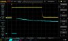
just the -10 deg signal. the setup ran fine inside at 20 HZ / 1200RPM.
using the fct. gen w/ a sine-wave output.
and both Q1 and Q2 were mildly warm after a 2-min. run . they were both
monitored carefully as neither one has a heat-sink mounted to it.

the first foto shows the whole test setup outdoors. the engine would be spun up using the big 12 V.
car battery. and the cycle's starter motor. tho it was not 'scoped for verification this should have resulted
in the flywheel signal being produced. there's no reason for it to not be there. and , yes, this is
an assumption that will need verified. esp. now that reasons for not getting a spark are sought

all i hoped for was to see was a spark on the plug hanging off the board. you can see the plug there
below the blue 3S1P lithium battery pack in the 2'd foto. the 6" red wire runs from the plug's tip back to the ignition coil as a ground return.

the 2'd foto is a close-up of a piece of 1/8" paneling on which is mounted the CDI ckt bd , with the 2-Q ckt bd
screwed atop it with stand-offs. and the ignition coil, and 2 battery packs : one,12V, for the CDI ckt bd.
and the other, 5V , for the 2-Q ckt bd. in my hand is the 2-wire cable coming from the flywheel sensor coil.

Q2 is the n-FET that acts as a switch. when it 'closes' the charge stored at 300V in C2
passes thru it on the way to the primary of the igntion coil. in foto 2 , at the CDI ckt bd it is
standing upright at the top side of the board. a 3-legged TO-252 package. that green thing
at its bottom is a screw-connector to fasten it to the ckt bd. no soldering necessary. this is
a change in the 2014 design. makes for easier replacement of the n-FETs as they are
more likely to fail than about anything else.

the outdoor test result was NO spark and one hot Q2. and a new interesting problem to figure out. why is Q2 getting hot and no spark happening ?

one idea to persue is this. the 2-Q circuit runs on 5V. and if it runs as well on 12V. then
the circuit of the 7-1-16 post can be simplified. and no need for a 5V-to-12V interface Q exists any longer.
plus we'll just let U2 clean up the slope with its Schmitt input.
 
Last edited:

bob weir

Sep 10, 2014
235
Joined
Sep 10, 2014
Messages
235
hey guys , the CDI design you've seen here all along is being set aside. its been giving me fits.
and needs problematic re-work to interface to. so another , simpler circuit, was searched for.
and its one we're already near familiar with ( see posting june 21 '15). and now its at the center of my attention. so far the experiments have been encouraging. its txfr has a 12.5:1 turns ratio, and ours is 10:1 so will likely substitute nicely. and the firing switch is a SCR not a n-FET thus no mosfet driver IC is needed. a big unknown at this point is whether the IRFZ44n FET or the
BT151 SCR will need heat sinks.

give this link a look. and consider what the advantages are to use a CDI based on the UC3845. its looking like having many parts of the former circuit embedded in a single IC.

http://www.sportdevices.com/ignition/inverter.htm

a number of companies make this chip. here's a link to the data for one of them.
reading it will help to understand how the Sportdevices people set up the circuit.
and how to deal with the Vfb and Is pins. out uC will send a signal to the Is pin
to stop the oscillator and another to the SCR to next fire the plug.

http://www.microsemi.com/document-portal/doc_view/11286-uc184xa-pdf
 
Last edited:

bob weir

Sep 10, 2014
235
Joined
Sep 10, 2014
Messages
235
today a small study. of the coil inside the flywheel. to look at the signals it provides us
for the timing of the spark.

first is a sketch of the circuit and how the scope is connected.

and last is the scope image. taken as the engine spun via the starter motor at about 500 RPM

playing with the load resistor led to learning the largest amplitude was at about 2500 ohms.

also see that the 2 lobes are pretty symmetric. and equal amplitude.
flywheel signal  R = 2500 july 11 001.jpg flywheel signal and R 2500               july 11 2016.jpg
 
Top