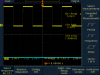
Channel 1 = input signal (at base of transistor)
This can't be. The base of the transistor will not rise much above ~0.6 V ... 0.7 V. At that voltage the base-emitter diode becomes conducting and the resulting base emitter current will drop the rest of the input voltage across the series resistor from signal source to base. Your scope signal shows ~ 5 V signal level, thus you surely are measuring at the signal source or the left side of the series resistor, not at the base of the transistor.
when connected to the base of the transistor, the input signal drops about 0.4Volt
Your signal source is very probably far from an ideal voltage source. It will have some internal resistance.
When the input voltage is high, the transistor is conducting. The input current to the circuit is approx. 400µA as calculated from:
(5 V from the signal source - 0.6 V base emitter voltage -0,4 V voltage drop observed)/10 kΩ.
A current 0f 400 µA and a voltage drop of 0.4 V correspond to an internal resistance of the source of ~ 1 kΩ.
You can check this by replacing the 10 kΩ series resistir by e.g. a 1 kΩ series resistor. The voltage drop will be much higher due to the higher input current. Expect about 2 V ... 2.5 V drop in that scenario.
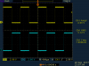
Picture 2 = with collector to gnd
Picture 3 = with emitter to gnd.
When you operate an NPN transistor with collector to ground, it will seem to work regardless of the mixed up connections. This is called reverse mode of operation.
However, the current gain is greatly reduced. An easy explanation you may
read up here.

")
